4 bit ripple carry adder pdf editor

This implies that the inputs to the logic must be the propagate and generate signals of the full adders. By combining the 4 blocks and a bit adder can be implemented. The first block LSB is a full adder by itself. The design of a carry-skip adder is based on the classical definition of generate and propagate signals as follows [ 12 ]:

The adder was implemented by dividing the adder into several blocks. The lowest-level subblock is formed by a number of variable width RCAs. The main principle behind this design was to utilize the lower blocks and make them work in parallel with higher blocks.

They divided the n-bit adder into ascending and descending halves so as to limit the number of bits in the final stage. A block diagram of with an expanded view of subblock is shown in Figure 4. The lowest-level subblock is formed by a number of variable width RCAs. RCA was concluded to have utilized the least power, but has the highest delay due to its carry chain.

Introduction The ever-increasing demand for mobile electronic devices requires the use of power-efficient VLSI circuits. Figure 5 shows block with an expanded view of subblock The number of RCAs in is limited to 3 due to the condition stated earlier. The first one is referred here as Chirca adder and the second one is referred as Gayles adder. MHz and is also shown in Table 2.
The area used is. They emphasized the need for regularity in VLSI circuits to reduce design and implementation costs. This implies that the inputs to the logic must be the propagate and generate signals of the full adders.
Now consider block in Figure 2. The carry input to the final subblock is given by. On the other hand, when the generate-propagate outputs are used for group generation and group propagation outputs, a stack height of 3 in the CMOS implementation will allow a 4-bit RCA. The ELM-adder design presented in [ 7 ] computes the sum bits in parallel; thereby reducing the number of interconnects. Although our adder has already achieved the bit requirement, we still have room to extend the width further, while keeping the target delay the same.

Hence, the number of RCAs in any subblock is limited either by the number of inputs to the CG block or by the number of inputs to the block. The average power was measured by feeding 10, random vectors at a frequency of ? The simulation results are shown in Table 3. The number of inputs to the CG logic increases, successively, by 2 for each RCA and is limited to a maximum of 7 in any subblock. To get a more realistic estimation of the delays involved, we laid out the complete bit adder stages 4 bit ripple carry adder pdf editor performed TSPICE simulation.

To reduce delay and power consumption, the adder is divided into variable-sized blocks that balance the inputs to the carry chain. Addition is the most basic arithmetic operation; and adder is the most fundamental arithmetic component of the processor. Hence, the total width of block is 19 bits.

The algorithm ends up in an unbalanced binary tree with a delay of consuming an area. The group generate and group propagate functions are generated in parallel with the carry generation for each block. A bit adder implementation with a delay of 7 logic levels using carry-skip adders and ripple-carry adders was presented in [ 4 ]. 4 bit ripple carry adder pdf editor ELM-adder design presented in [ 7 ] computes the sum bits in parallel; thereby reducing the number of interconnects.
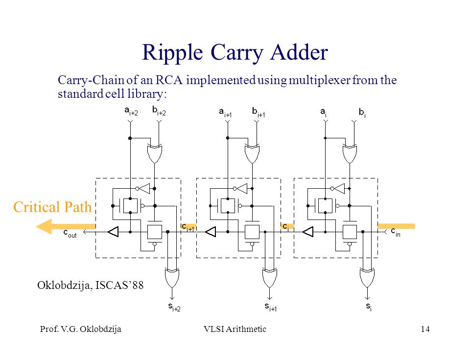
The 4 bit ripple carry adder pdf editor block is a single bit full adder. Although our adder has already achieved the bit requirement, we still have room to extend the width further, while keeping the target delay the same. The ripple-carry adder RCA is the simplest adder, but it has the longest delay because every sum output needs to wait for the carry-in from the previous full-adder cell. This implies that the inputs to the logic must be the propagate and generate signals of the full adders. In our design, the generate-propagate logic balances the delay and the number of inputs to the skip logic limits the critical path delay.